Loading
Introduce the product here. A small description about what it is and how it helps the user. You can also add some photos below.
The structure of Silicon on Insulator (SOI) wafers—Silicon (top) / Insulator (SiO₂) / Silicon (substrate)—is a defining feature that distinguishes SOI from traditional bulk silicon wafers.

This is a thin, high-quality single-crystal silicon layer where active devices, such as transistors, are fabricated. Its thickness typically ranges from a few nanometers to several micrometers, depending on the application (e.g., fully depleted or partially depleted SOI).

This is a buried oxide (BOX) layer, typically made of silicon dioxide (SiO₂), with a thickness ranging from tens of nanometers to a few micrometers. It acts as an electrical insulator between the top silicon and the substrate.

This is a thicker, bulk silicon layer that serves as the mechanical support for the wafer. It is typically several hundred micrometers thick and does not participate in the electrical operation of the devices.
List out your product’s benefit here. A small description about what it is and how it helps the user. You can also add some icons.
SOI technology enables fabrication of low leakage, low power integrated circuits for mobile devices
Ultra-fast switching RF SOI devices used in 5G, WiFi 6, and radar communication systems
SOI wafers are ideal for manufacturing ultra low-noise IF, RF semiconductor amplifiers
Rugged SOI chips meet automotive reliability and temperature requirements
SOI wafers are useful for integrating electronics and photonics for optical transceivers and sensors
SOI wafers are suitable substrates for specialized MEMS accelerometers, gyroscopes etc.
Customizability is a major cornerstone of WaferPro and we always try our best to meet all your needs. In that very essence WaferPro offers SOI wafers of the following types:
This type of wafer has device thickness from 1µm to 300µm.
This type of wafer has device thickness <500nm.
Uniformity of device thickness can be as low as ±0.5µm for thick SOI and ±10nm for ultra-thin SOI.
This type of SOI has very low BOW/WARP/TTV for specific applications.
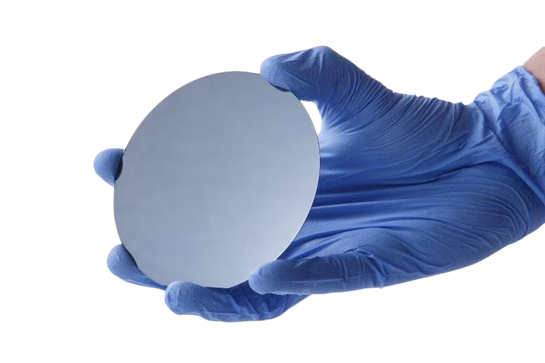
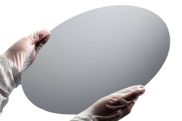
WaferPro now provides premium quality silicon-on-insulator (SOI) wafers, expanding our comprehensive silicon wafer offerings. Our top-tier SOI wafers are optimized for diverse applications from sensors to power components.
Chips fabricated on SOI wafers achieve 30% faster speeds and 80% lower power demands compared to CMOS devices. The SOI structure consists of three layers: a top active device layer for transistor fabrication, a buried oxide (BOX) insulator layer, and a bottom handle wafer layer.
The BOX insulates the delicate devices, shielding them from environmental interference while enhancing performance. Transistors built into the top device layer drive the speed and efficiency gains of SOI technology. They allow for sophisticated power-saving configurations and reduced data loss from cosmic rays or radiation.
With the addition of SOI wafers, WaferPro now delivers this advanced substrate option to R&D teams and manufacturers pursuing next-generation innovations. Our SOI wafers merge cutting-edge design potential with our proven wafer manufacturing quality.