P O W E N C Y

Loading

img

IC Packaging

Overview

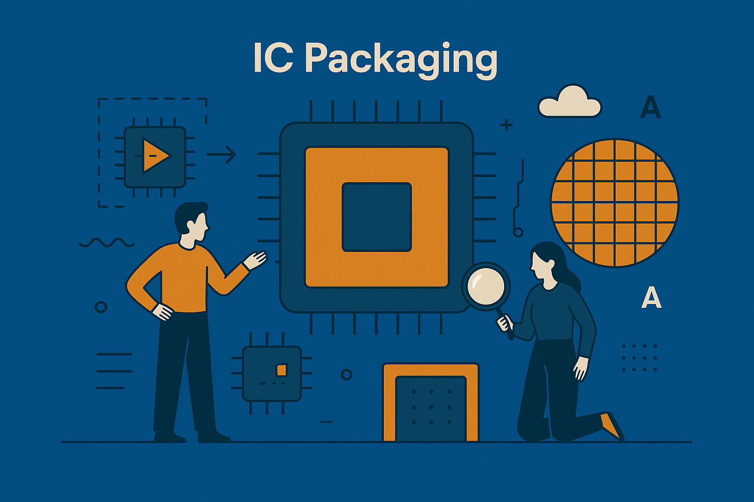
Integrated Circuit (IC) packaging is the process of enclosing a semiconductor chip in a protective housing that supports its operation and integration into larger electronic systems. It not only shields the chip from environmental factors like moisture and physical damage but also enables it to interface with the outside world through electrical connections and thermal management.

As semiconductor technologies evolve and shrink in size, packaging plays an increasingly critical role in maintaining the chip's reliability, performance, and longevity.

What We Offer

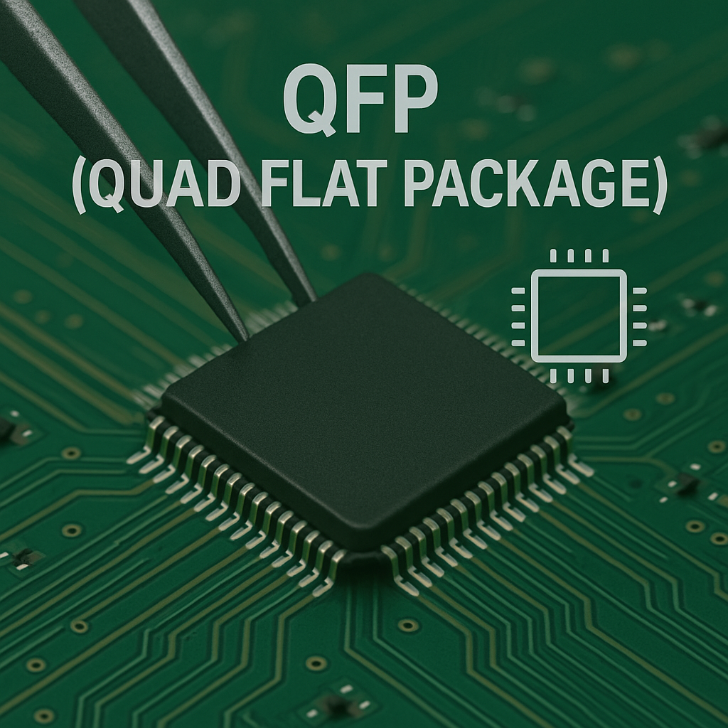
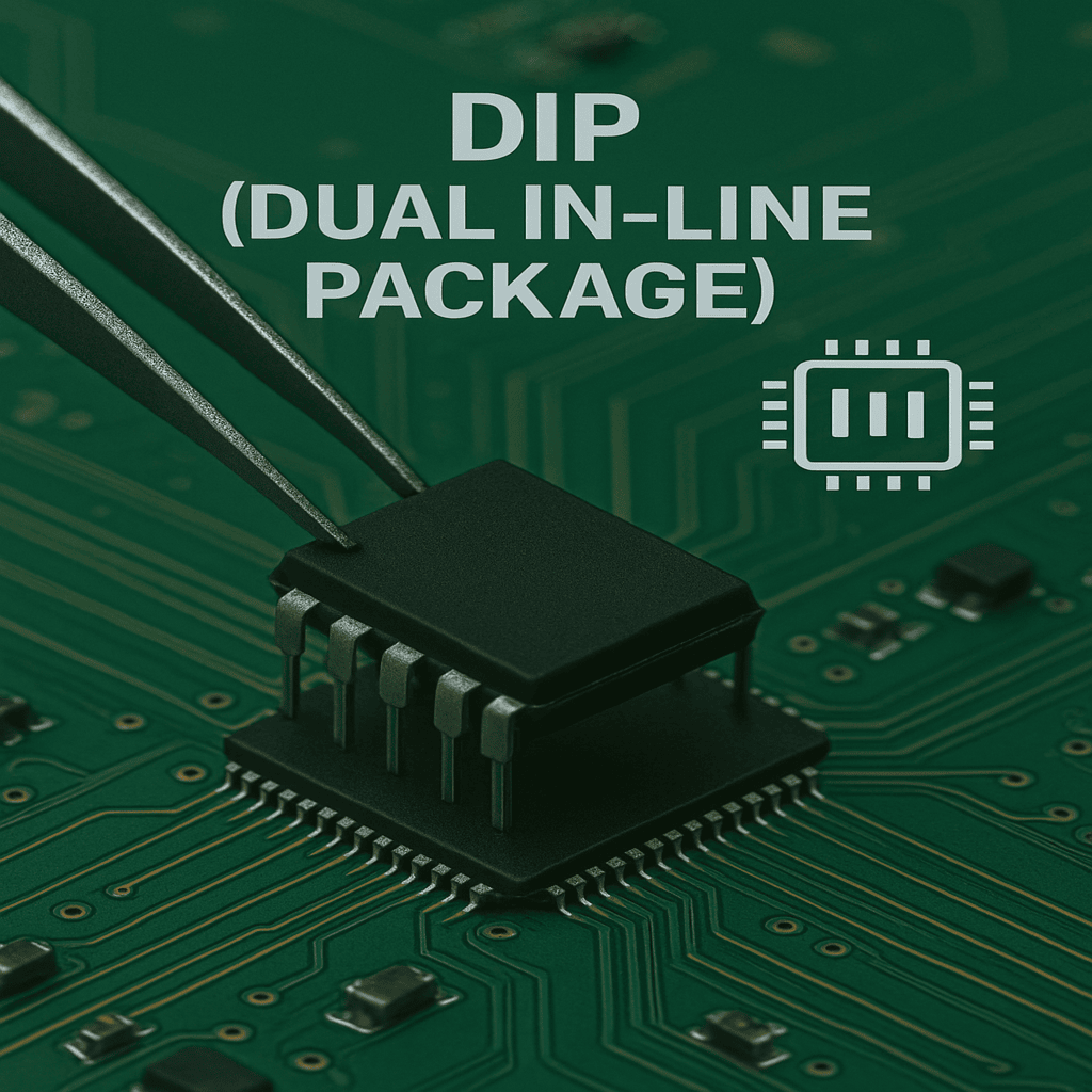
We provide customized IC packaging services tailored to your product’s requirements. Our capabilities include:

  • Advanced package design and layout
  • Thermal and electrical analysis
  • Material selection and stack-up optimization
  • Prototyping and testing support
  • Expertise across 2D, 2.5D, and 3D packaging technologies

Our team ensures your devices are ready for real-world deployment by focusing on functionality, durability, and manufacturability.

Industries We Serve

Our IC packaging solutions are designed to support a variety of industries, including:

  • Automotive electronics: High reliability under extreme conditions
  • Consumer electronics: Compact, cost-effective solutions
  • Industrial systems: Rugged packaging for harsh environments
  • Mobile and IoT devices: Space-saving, energy-efficient designs
  • High-performance computing: High-density, thermally-optimized packages

Why Partner With Us

Choosing us as your IC packaging partner means gaining:

  • Deep technical expertise in advanced packaging techniques
  • A commitment to quality and long-term performance
  • Experience with multiple packaging formats and technologies
  • A collaborative approach tailored to your product roadmap
  • Timely delivery and support throughout the product lifecycle

We focus on building solutions that fit your business goals — with precision, speed, and dependability.

Our Process

Our packaging process is comprehensive and detail-oriented, ensuring your chip performs as expected from design to deployment:

  • Requirements Gathering: Understanding performance, size, thermal, and cost targets
  • Package Design: Crafting custom layouts using industry best practices
  • Simulation & Analysis: Validating thermal, electrical, and mechanical behavior
  • Material Selection: Choosing substrates and encapsulants based on application needs
  • Prototyping & Testing: Ensuring the package meets reliability and compliance standards
  • Production Support: Guiding seamless transition from design to high-volume manufacturing
img
img

Most Comment Question?

Find answers to the most asked queries on IC packaging, from protective enclosures to thermal solutions in modern semiconductor design.

IC packaging serves as a protective housing for the silicon chip. It safeguards the chip from environmental damage, provides mechanical stability, enables electrical connections to external circuits, and helps manage heat dissipation during operation.
The choice depends on several factors such as application, power consumption, size, and thermal requirements. For example, BGA is often used for high-performance systems, while CSP is ideal for compact mobile devices. Design goals and system integration needs typically guide the package selection.
Modern trends include 3D packaging, system-in-package (SiP), fan-out wafer-level packaging (FOWLP), and advanced thermal solutions. These approaches aim to improve performance, reduce size, and support higher I/O density in today's miniaturized electronics.
Yes, significantly. A well-designed package can enhance signal integrity, ensure proper heat dissipation, and protect against physical damage — all of which contribute to long-term performance and reliability. Poor packaging, on the other hand, can lead to failures due to overheating or connection issues.