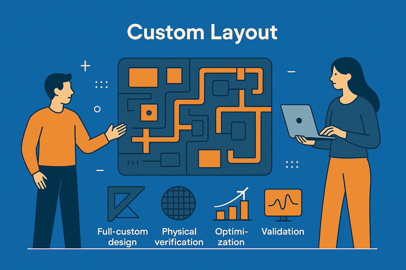
Custom Layout
Overview
In semiconductor development, achieving performance and reliability begins with precision in layout. Our layout design services support analog, RF, digital, and mixed-signal technologies, providing the foundation for high-efficiency, silicon-ready solutions. We help clients meet strict physical and electrical design goals with layouts optimized for manufacturability and performance.
What We Offer
- Custom Analog & RF Layout: Tailored layout for amplifiers, LDOs, ADCs, DACs, PLLs, and other precision circuits.
- Digital Layout Services: Custom datapaths, memory blocks, and cell-level layout optimized for speed and area.
- Design Compliance Checks: Full support for LVS, DRC, and DFM to help ensure first-pass silicon success.
- Process Porting: Migration and adaptation of layout IPs across various process nodes and foundry technologies.
Industries We Serve
- Automotive Electronics (ADAS, EV power management)
- Consumer Devices (mobile, audio, wearables)
- Medical Electronics (monitoring and diagnostic ICs)
- Industrial Controls (sensor front-ends, signal processing)
- Aerospace and Defense Systems (reliable analog/RF systems)
Why Partner With Us
- Proven experience with analog, RF, and digital layout
- Focus on accuracy, manufacturability, and performance
- Expertise in layout migration across technology nodes
- Collaborative workflow with design and verification teams
- Flexible engagement models for startups and enterprise clients
Our Process
- Requirement Discussion: We define key layout specs, process nodes, and area targets with your team.
- Floorplanning & Planning: Structured layout planning to align with hierarchy and performance goals.
- Layout Execution: Manual and semi-automated layout using industry-standard EDA tools.
- Verification & Signoff: DRC, LVS, and parasitic extraction to validate layout integrity.
- Handoff & Tape-Out: Delivering clean, verified layout data ready for fabrication.
Most Comment Question?
Discover clear answers to frequently asked questions about custom layout in semiconductor design. From layout techniques to performance benefits, find key insights into how precision layout shapes modern ICs.