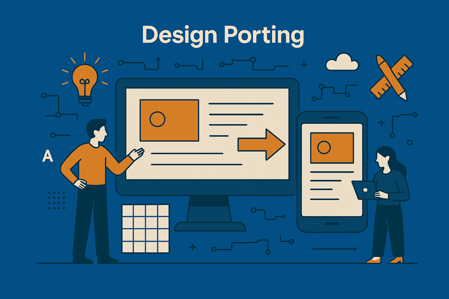
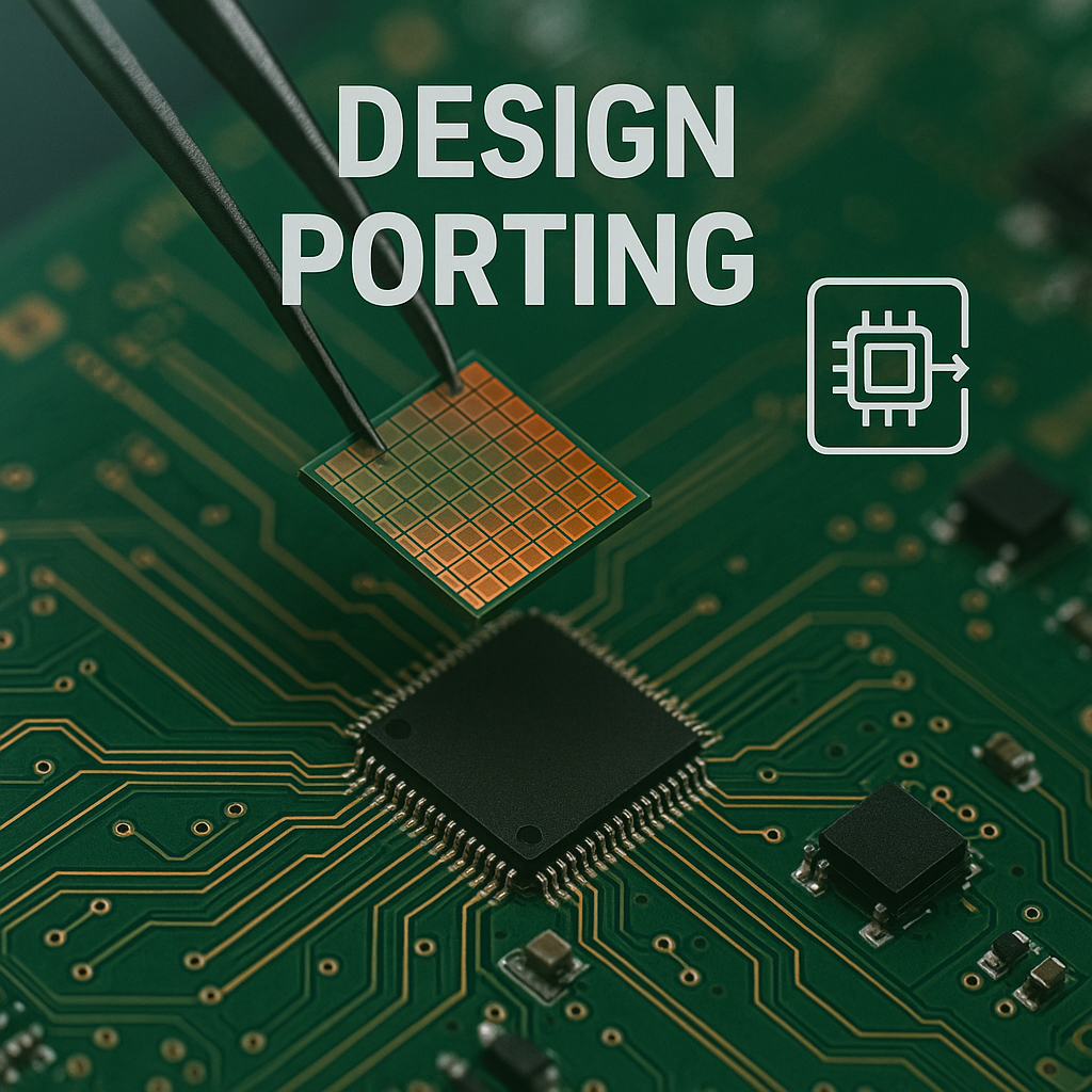
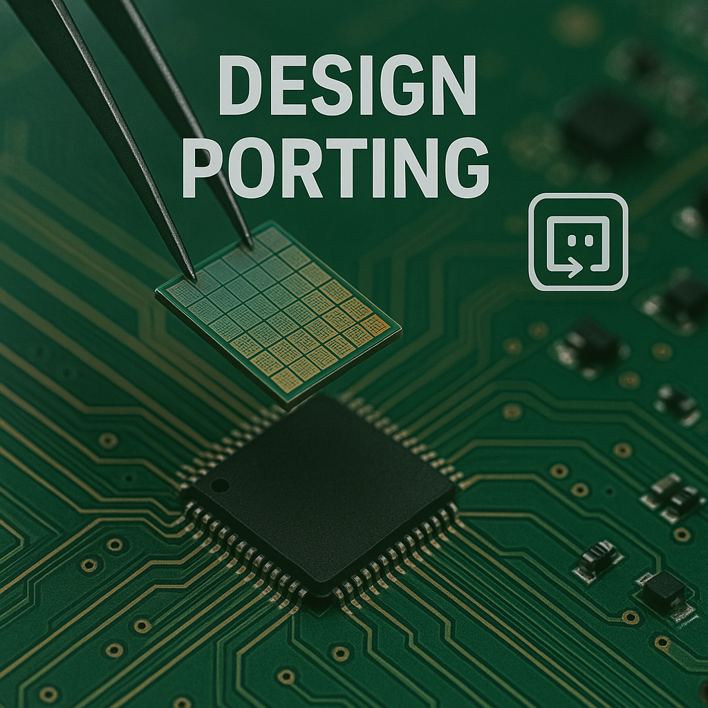
Design Porting in Semiconductor
Overview
Design porting is the process of adapting an existing integrated circuit (IC) design to function on a different semiconductor process node or foundry platform. As chip technologies advance rapidly, organizations often need to shift to smaller geometries or alternative fabrication environments. This transition ensures their products stay competitive, efficient, and manufacturable.
What We Offer
We provide complete design porting solutions to help businesses smoothly transition their semiconductor designs across platforms, technologies, and process nodes. Our services include:
- Migration between different nodes (e.g., 65nm to 28nm)
- Porting designs between foundries (e.g., TSMC to GlobalFoundries)
- Support for analog, digital, and mixed-signal designs
- Adaptation for both ASIC and SoC platforms
- Optimization for power, area, performance, and yield
Industries We Serve
- Consumer Electronics
- Automotive Semiconductors
- Telecommunications
- Healthcare & Medical Devices
- Industrial Automation
- Aerospace and Defense
Why Partner With Us
- Extensive Domain Knowledge – Deep understanding of multi-node and multi-foundry porting challenges
- Process-Agnostic Expertise – Ability to work across major semiconductor platforms and foundries
- Risk Reduction – Thorough verification and validation at every stage of the porting lifecycle
- Faster Time-to-Market – Accelerated porting using proven methodologies and automation tools
- Collaborative Engagement – Transparent communication and iterative feedback at each phase
Our Process
- Design Review – Understand the current architecture, constraints, and process dependencies
- Library & IP Mapping – Identify compatible components in the new target node
- Constraint Optimization – Update timing, power, and area targets as per new specifications
- Layout Redesign – Modify the circuit layout to comply with the new technology’s rules
- Validation & Sign-off – Run comprehensive DRC, LVS, and functional simulations to ensure design integrity
Most Comment Question?
Get clear answers to key questions about migrating your chip designs across process nodes and technologies — for better performance, scalability, and time-to-market advantage.